
- This event has passed.
Ballistic Electron-Emission Microscopy (BEEM) : from the local electronic properties to magnetic imaging
December 14 , 13:00 – 14:00
Speaker: Dr. Pascal Turban
Affiliation: Institute of Physics, Rennes University-CNRS, France
Link to the MSTeams meeting
Meeting ID: 326 783 705 625
Passcode: 2Up2Lt
Download Teams | Join on the web
Ballistic electron-emission microscopy (BEEM) is an experimental technique measuring the electron current which, injected from the tip of a scanning tunneling microscope (STM) into a thin metallic overlayer, travels through an underlying metal-semiconductor (MS) interface and is finally collected in the semiconductor substrate. Given the current trend in the development of electronic devices at the nanometer scale, BEEM is a powerful tool for the nanoscale characterization of electron transport through various MS heterostructures. In this talk, I will illustrate some specific potentialities of BEEM for the study of ultrathin metallic films and nanostructures epitaxially grown on III-V semiconductors:
- For simple single-crystalline Schottky contacts, the structural continuity at the epitaxial interface results in the conservation of the electron transverse momentum k// at the MS interface. Due to this transverse momentum conservation rule, BEEM is highly sensitive to the local MS interface electronic structure.
- For Fe/Au/Fe/GaAs(001) epitaxial spin-valves, the measured hot-electron current is strongly modulated by the application of an external magnetic field. This magnetoresistance amplitude reaches 500% at room-temperature and can be explained by taking into account the previous electronic selection rules at each interface of the heterostructure generalized for both up and down spin channels.
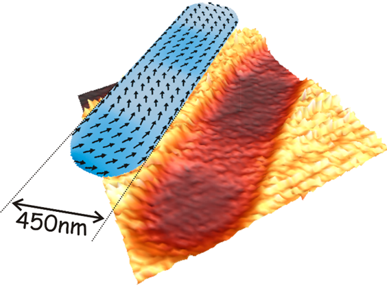
- Finally, the large magnetoresistance amplitude achieved in these spin-valves allows the observation of magnetic domains in the Fe electrodes. The performances of BEEM as a magnetic imaging technique with strong contrast and subnanometer lateral resolution are demonstrated on patterned sub-micronic Fe/Au/Fe(001) spin-valves.
Chairman: Prof. Jarosław W. Kłos